AMD Strikes Back: Zen 5 CPU Architecture Changes & Chipset Differences (X870E vs. X870, B850, B840) Leave a comment
Overview
We’ll get proper into the fast details first – a few of this we already lined from AMD’s Computex announcement, however some is new info. Sadly we don’t have value info to share on the time of writing.
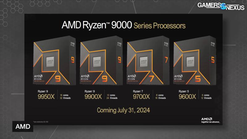
AMD’s Ryzen 9000 desktop CPUs are codenamed Granite Ridge, function the Zen 5 structure, and are nonetheless on the AM5 socket. This primary picture might be a recap of issues we already knew, adopted by new architectural info.
The recap exhibits that the lineup is basically similar to the preliminary Ryzen 7000 CPUs. The flagship Ryzen 9 9950X has 16 cores, a 5.7GHz max enhance, 80MB of cache, and a 170W TDP. Down from that’s the Ryzen 9 9900X with 12 cores, barely decrease enhance and cache, and a 120W TDP. Then the Ryzen 7 9700X with 8 cores, 5.5GHz max enhance, a smaller 40MB cache on account of being single-CCD, and 65W TDP. Lastly, the 6-core Ryzen 5 9600X holds up the underside of the stack.
Notably, the TDPs for the underside 3 are down considerably versus their Ryzen 7000 counterparts. As a reminder, TDP doesn’t equate to energy consumption and isn’t constant throughout distributors and even throughout sockets. AMD’s Bundle Energy Monitoring (PPT) is a extra helpful energy consumption guidepost, however we don’t formally have these for Ryzen 9000 but.
We requested AMD if the TDP components and HSF thermal resistance values are the identical for this collection as 7000. AMD confirmed that the comparisons are like-for-like; nonetheless, precise energy consumption will nonetheless range considerably. A method that may range is from discount within the precise warmth, which ought to scale back energy leakage.

AMD claims it has improved the thermal resistance by 15% for a 7-degree discount at equal TDP. We requested AMD the place this enchancment got here from: The corporate informed us that the development is basically from sensor placement optimization, or transferring the precise temperature sensors to raised places on the die. Which means that the Tdie worth might be decrease, which AMD says provides it extra headroom for reinforcing.
Zen 5 Structure
AMD gave press a deeper dive into its architectural modifications for Zen 5, and it’s positioning it as a spot to develop from.
On the occasion, AMD CTO Mark Papermaster acknowledged, “It actually represents an enormous leap ahead, and in reality, it’s going to be a pedestal that we’re going to construct upon the following a number of generations of Zen.”

AMD redesigned key parts of the entrance finish, together with fetch, decode, and dispatch. This offers extra directions to the again finish each clock tick. Zen 5 has wider execution pipelines to execute the directions. AMD says that effectivity will increase from improved cache with extra bandwidth and an expanded execution window, which the corporate states is meant to keep away from execution stalls.

Shifting into extra element and beginning on the entrance finish with pipe fetch, department prediction is decrease latency, extra correct, and with extra predictions per cycle in Zen 5, in response to AMD. This all provides as much as extra throughput within the entrance finish. Downstream, Zen 5 has twin ported instruction cache and op cache, whereas reducing latency. AMD additionally added a twin decode path.

Subsequent is dispatch and the execution engine. Zen 5 options 8-wide dispatch and retire, 6 ALUs with 3 multiplies, and a extra unified ALU scheduler (there was a singular scheduler for every of the ALUs).
Papermaster went on to say, “We then went from the truth that we had these wider execution pipelines, realizing that when you may have extra directions that you just’re dealing with, you must take into consideration dealing with misses successfully and holding the efficiency of these execution pipelines. Once more, hardcore micro-architecture engineering.”
AMD additionally expanded Zen 5’s execution window by 40% with as much as 448 supported OPs, which AMD says is a big driver of extra efficiency. Zen 5 additionally has a bigger 48KB information cache, up from 32KB on Zen4, and double the utmost bandwidth to the L1 cache and Floating-Level Unit, and improved information prefetching.
Papermaster acknowledged, “While you develop caches like that, what sometimes occurs is you run a excessive threat of accelerating the latency. You grew the cache, that is usually going to occur. However what we did on this case, the staff simply did an outstanding job. And they also maintained really that four-cycle entry that we had had regardless of the expansion, the 50 p.c progress within the information cache. With Zen 5, we are able to now execute 4 hundreds per cycle.”

The ultimate key enchancment AMD made relating to information bandwidth is to information prefetching, the place AMD says that tuned algorithms give far more stride sample recognition.

Subsequent are the floating level and vector math unit enhancements. These embody a full 512-bit information path, 6 pipelines with two-cycle latency FADD (floating add), and a bigger variety of floating-point directions in flight at one time.
Papermaster acknowledged, “So I talked about that 512-bit information path. That is extra necessary than ever. As a result of when you consider it, there’s been no discount within the type of math-hungry workloads of gaming, of HPC, of content material creation. So when you consider these customers of the maths unit, none of them are going away. However AI with its want is now turning into a workload in all places.”

AMD has up to now carried out AVX-512 by double-pumping a 256-bit pipeline, which made positive that the CPU wouldn’t should drop clocks whereas doing AVX-512 workloads. With Zen 5, AMD engineered a option to help full frequency whereas working the bodily information path at true 512-bit. Our understanding is that that is modular to the extent that the older double-pump strategy continues to be potential in some conditions if the corporate needs to construct it that means.
Zen 5 additionally lowers the latency of floating-point operations from 3 cycles to 2.
Papermaster acknowledged, “So we doubled the bodily pipeline, we lowered the latency, we’ve elevated the throughput. And that, mixed with the load/retailer enhancements that I described, actually create an excellent optimized engine throughout these workloads I described – AI, HPC, gaming, content material creation.”

All of those enhancements bundled collectively end result within the claimed 16% common geomean uplift in IPC versus Zen 4, with as much as 35% single core uplift in AES-XTS encryption.

The breakdown of Zen 5’s uplift consists of knowledge bandwidth, fetch/department prediction, execution/retire, and decode/opcache enhancements.

In a extra bodily sense, Zen 5 strikes to 4nm and 3nm course of know-how with an enhanced steel stack for greater efficiency and decrease resistance.

Ryzen 9000 Efficiency Claims
AMD shared first-party efficiency claims that centered on IPC enhancements – one thing AMD needed to make very clear for the reason that listed max enhance frequencies aren’t transferring a lot, if in any respect. We gained’t spend an excessive amount of time right here, since we’ll have our personal full testing for every CPU, and it’s by no means good to blindly belief the producer’s personal benchmarks. It will at the least set expectations. Our assessment will run close to launch.

In keeping with AMD, the primary set of checks had been carried out with matched clocks between a 9950X and 7700X. Claimed IPC uplift ranged from as much as 10% in Far Cry 6, to 23% in Blender. Geekbench 5.4 was even greater, however looks as if a possible outlier.
We’d have most well-liked if these had been carried out with matched core counts, as AMD is mainly asking us to increase the advantage of the doubt that the checks weren’t set as much as give a bonus to the CPU with a bodily {hardware} benefit.

Shifting on to AMD’s aggressive testing, it matched up the 12-core 9900X versus Intel’s 14900K, claiming a 41% enchancment in Handbrake, 22% in Horizon Zero Daybreak, and 4% in Borderlands 3.

AMD additionally in contrast its 9700X to the 14700K, citing a 19% benefit in Puget’s Photoshop benchmark, which we’ll run in our assessment, and recreation benchmarks that ranged between 4% and 31% within the 9700X’s favor.

Then lastly transferring on to the 9600X, AMD matched it in opposition to the 14600K. There’s a large 94% win in Handbrake, together with a smattering of different productiveness and gaming wins.
Evaluating its former AM4 king, AMD ran the 9700X versus the 5800X3D the place it claims a mean 12% sooner geomean. That may very well be an enormous effectivity win as nicely, however we’ll want to check it.
AMD SOC Structure Panel

On the finish of AMD’s occasion, it held an SOC structure panel with 4 of its Fellows that had some actually attention-grabbing insights into varied facets of AMD’s design and course of and strategy. These are 4 engineers on the firm. Mike Clark is the Chief Architect of Zen and its originator, Will Harris is a platform engineer and is aware of the chipset and socket, Mahesh Subramony is a silicon design engineer, and Joe Macri is the computing & graphics CTO.

One of many early questions needed to do with the truth that AMD is rolling out heterogeneous core architectures in a few of its merchandise. There was a humorous slip — or perhaps not — from computing & graphics CTO Joe Macri, “Mahesh, you understand, after we take a look at our competitors, Intel, you understand, they’ve a efficiency core, an financial system core.” There have been some stifled laughs within the crowd from that one — it comes throughout as a dig at what Intel calls the “environment friendly” core.
Macri additionally acknowledged, “You already know, now we have heterogeneous cores additionally. Our philosophy is totally different in how we strategy desktop or cellular.” Turning to Mahesh Subramony, Macri requested, “Perhaps you could possibly, you understand, dive in somewhat bit there and clarify, you understand, why two corporations which might be aiming on the identical markets strategy issues simply so in a different way.”

AMD Senior Fellow and Silicon Design Engineer Mahesh Subramony replied, “It truly is microarchitecture actual, ISA actual, and IPC actual modular, the cache dimension it attaches to. So the heterogeneity, if you’ll, is de facto across the voltage frequency response. So giving up a few of that peak, frequency peak efficiency and get a few of that again in space and effectivity. So that is what the compact core does for us. The desktop consumer calls for efficiency, low latency and throughput for each process they need to do. So they’re higher served with a homogenous traditional core with a greater efficiency, if you’ll, and a voltage frequency response, if you’ll, dynamic. And on the cellular facet, despite the fact that they don’t seem to be that far behind of their compute necessities, they care lots about energy effectivity. And that is the place the compact core type of suits proper in. A right combination of the traditional and the compact cores delivers that scalability in efficiency with out compromising on the ability effectivity.”
Macri added that since AMD’s compact cores are in essence the identical as common cores, it makes issues simpler from an OS software program perspective, “The nook circumstances that you just expertise once you obtained cores which might be very separate of their attributes simply confound the consumer, make that consumer expertise tougher, make the OS companions have a tougher life.”
These are attention-grabbing phrases from the corporate that shipped the 7950X3D and 7900X3D – CPUs with totally different efficiency traits ensuing from having one CCD with stacked V-Cache and decrease core frequency, and the opposite with out the additional cache however greater core frequency. These CPUs open up a can of worms that, in an effort to get the most effective efficiency in all circumstances, require particular drivers and even consumer information and intervention that we might classify as confounding.

Macri then addressed AMD Fellow and Platform & Techniques Structure Will Harris, citing the AM5 platform, its socket, and longevity – stating that AMD intends for AM5 to last as long as 7 years. Will Harris, AMD Fellow of Platform and System Structure responded by saying, “And so one of many first issues that we do as we’re designing a brand new infrastructure, equivalent to AM4, AM5, is we type of tie it to a serious interface that is transitioning. So, usually, it is often reminiscence, for instance. So AM4 was tied with DDR4, and AM5 was tied with DDR5.” Harris added, “…And such as you mentioned, we wish that longevity, so then we do issues like ensuring that now we have enough interfaces to go for a number of generations. We be sure that we have got the sign integrity, isolation on the pins on the package deal, in order that we are able to get a number of pace bumps and enchancment over time on issues like reminiscence speeds or PCI Specific speeds, for instance.”
Harris additionally mentioned AMD evaluates trade developments, requirements committees, and third occasion distributors to see the place the market is heading extra long-term.
Subramony then jumped in, saying that with generational positive factors in the identical die space slowing down, AMD has so as to add die dimension in an effort to get extra substantial positive factors in IPC and whole efficiency. If the dies get bigger, they nonetheless want to suit on the identical bodily package deal – a troublesome problem throughout a number of generations. Macri responded, “And, you understand, the staff has to dive in on the system physics stage, proper, the method know-how as we shrink it, you understand, voltages need to come down, however the platform has to remain constant.”
Macri took the chance to get in one other shot at Intel, “You do not have to go change your motherboard each different technology like another of us do.”
Truthful sufficient, so long as AMD doesn’t begin doing that in some unspecified time in the future. We’re good to at the least 2027, in response to AMD.
The dialog then turned to Simultaneous Multi-Threading, or SMT, addressing Intel abandoning Hyper-Threading on the upcoming P-cores in Lunar Lake.

On the occasion, AMD Company Fellow and Silicon Design Engineer Mike Clark acknowledged, “Yeah, so I feel as we talked about heterogeneity earlier, you understand, with Intel having two core sorts, one with SMT and one with out, I can positively see how that will be actually laborious to handle for software program. So I am unable to actually remark extra on their design decisions, however that looks as if an apparent one that stands proud.”
Once more, AMD’s 7950X3D is correct there staring us within the face with the identical scheduling issues, however Clark continued, addressing the precise matter at hand, “For us, I imply, SMT is the most effective perf per watt per space function that now we have. …Implementation does matter, too, so you must do it in a really sensible means, similar to all of the microarchitectural options, you understand, Mark rolled out yesterday. And so for us, you understand, SMT is a couple of 5 to 10 p.c space hit versus, you understand, workload enhancements that go from 20 to 50 p.c.”
Clark then acknowledged that SMT doesn’t work in each situation, and that if a workload is bandwidth intensive, having extra cores gained’t assist greater than having SMT. AMD makes some processors with SMT off, and it permits the tip consumer to show it off.
In addition they briefly mentioned future Zen 6 and Zen 7 CPUs, nevertheless it was restricted to the truth that AMD views Zen 5 as the brand new start line for the architectures to come back, in the identical means that Zen 1 was for its subsequent generations.
Chipset Variations

AMD is launching 4 new chipsets within the instant future: X870E (a 2-die resolution), X870, B850, and B840.

This desk simplifies it. AMD’s X870E and X870 chipsets will each run PCIe Gen5 to graphics and NVME. This can be a laborious requirement, as we perceive it, that the motherboard distributors should comply with. Each will even help USB4 as a requirement, CPU and reminiscence overclocking, and run 1x PCIe Gen5 x16 graphics slots or can run 2x 8-lane configurations.
AMD’s X870E chipset will use 2x Promontory 21 dies and retains the dual-chipset silicon format of X670E. All the pieces else makes use of a single chipset. This enables one of many chipset dies to be nearer to the PCIe slots, which could be helpful in hint routing. It additionally expands the final goal PCIe lane rely. B850 drops to Gen4 on the laborious requirement for graphics, however can use Gen5 for graphics. USB3.2 at 20Gbps can also be required. B840 is successfully an A-series chipset, just like the prior A320, besides rebranded presumably to both trick confusers deliberately or to simply trigger pointless confusion and havoc available in the market. This can be a low-end chipset that cuts-off at PCIe Gen3, runs USB 3.2 10Gbps, and removes CPU OC help. It additionally solely has 1×16 graphics slots.
The first distinction between X870E, X870, and the prior X670E and X670 boards is USB4 help. There could also be different significant modifications like availability of curve shaper, however a few of these particulars aren’t finalized but.

Right here’s a full table from AMD.
Common Function PCIe lanes could be assigned anyplace on the board and are allotted by the motherboard producer, however made obtainable by the chipset. Ryzen CPU mixtures with X870E will help as much as 44 PCIe lanes, in opposition to 36 whole on X870. Each help as much as 24 PCIe 5.0 lanes. X670E additionally runs 44 PCIe lanes and 24 as much as PCIe 5.0 whole. X670 drops to 44 and eight. B850 and B840 aren’t on this desk but.
B840 is successfully an A-series chipset. If you happen to’re going to purchase it, simply remember that B840 is just not just like B850 — it’s a giant step down.